Ledfocus Precision manufacturing
One-stop SMT/PCBA/OEM electronic contract manufacturing service provider

0755-83734236
0755-83734215
0755-29727486
0755-83734215
0755-29727486
- search keyword:
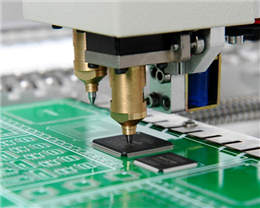
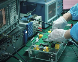
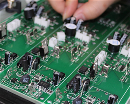
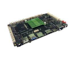
- PCBA proofing
- PCBA processing
- SMT foundry
- PCBA plate making
- SMT patch
- SMD ODM foundry